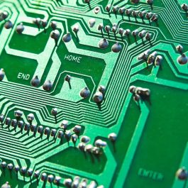
The electronics industry’s explosive growth has been fueling PCB evolution for years, constantly pushing for smaller, lighter boards that are more powerful than their predecessors. From cell phones to home automation systems, consumers expect more in sleeker packaging. As a result, the demand for multilayer PCBs has been skyrocketing. Multilayer PCBs are compact and lightweight, but offer sophisticated functionality.
What are Multilayer PCBs?
Multilayer boards consist of at least three layers of conductive material set in the middle with other layers stacked upon this core. The number of additional layers is determined by the complexity of the product. For example, smartphones often use 12 layers due to the various demands of the circuit. It is recommended to stick to an even number of layers as odd layers can lead to issues such as warping and twisting after soldering. While multilayer PCBs have higher manufacturing costs and more difficult repairs, their increased functionality make them a wise investment for complex electronics.
How are Multilayer PCBs Produced?
To produce multilayer PCBs, alternating layers of prepreg and core materials are combined into a single unit. Heat and high pressure are used to ensure uniform encapsulation of conductors, proper curing of the adhesives that bind the layers, and elimination of air between layers. With multiple layers of material, drill holes must be carefully observed and executed. Engineers must also incorporate a symmetrical layout across the layers to avoid twisting or bowing in the materials once heat and pressure are applied.
Benefits of Multilayer PCBs
The greatest benefit of multilayer PCBs is the space savings they offer, but other benefits include:
- Multiple layers of wiring for increased flexibility
- Decreased electromagnetic interference through careful placement of power and ground layers
- Reduced need for interconnection through wire harnesses, cutting overall weight
- Higher assembly density provides increased performance and functionality
- Available in both rigid and flexible construction (although the more layers incorporated, the less flexible the PCB becomes)
Multilayer PCB Applications
- Computers
- GPS technology
- Satellite systems
- Cell phones
- Heart monitors
- X-ray equipment
- Central fire alarm systems
Choose Telan as Your Multilayer PCB Assembly Service
Multilayer PCBs require precise engineering and careful assembly in order to meet all functional, performance, and reliability expectations. Telan has producing PCBs for over 35 years in accordance with the highest industry standards. Whether you are looking to produce three or 30 layer PCBs, Telan has the equipment and expertise to get the job done. Call us today at 215-997-7603 to learn more about our multilayer PCB services.


